Challenges Faced During PCB Assembly
A successful PCB assembly process requires meticulous planning and precise execution. However, due to factors such as faulty design data and poor thermal management, a number of challenges can arise that threaten the integrity of the circuit board. Luckily, these six common challenges faced during pcb assembly can be addressed by understanding the underlying causes and implementing the right solutions.
1. Incorrect Bill of Materials (BOM): Inaccurate BOM data can result in procuring incorrect components and assembling them on the circuit board. To avoid this issue, it is essential to collaborate with reputable component suppliers and implement stringent quality assurance processes.
2. Thermal issues: Improper heat management can lead to a number of thermal defects, including pad lifting and solder bridges. To mitigate these problems, it’s vital to test the thermal properties of the PCB before submitting it for assembly. Performing tests such as micro-sectioning analysis and cross sectioning can help identify and resolve any thermal issues that may impact the assembly process.
3. Overlapping components: Incorrect placement of components is a common error during pcb assembly. To prevent this, it is important to follow best practices for PCB layout and ensure that the design meets DFM (design for manufacturability) standards. This involves using appropriate footprint sizes, ensuring that there are sufficient clearances between components, and placing all necessary fiducial markers on the PCB.
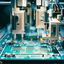
Six Common Challenges Faced During PCB Assembly
4. Component burning: If a component is exposed to extreme heat, it can burn and damage the circuit board, requiring costly repairs or even an entire board overhaul. To prevent this, manufacturers should use components that have a lower Tg (glass transition temperature) and operating temperature than the PCB. They should also ensure that the PCB is adequately spaced to allow the components to cool down without damaging adjacent parts.
5. Non wet open defects: Non wet open defects are a type of soldering issue that can occur when the copper on a pad is exposed, causing a short. This is usually caused by poor soldering skills or design errors, and can be avoided by ensuring that the appropriate settings are applied during PCB production.
6. Lack of space to work: Insufficient workspace makes it difficult for rework technicians to install new components, repair other assembly defects, and conduct thorough visual inspections. This can add up to a significant amount of waste and expense for manufacturers, so it’s crucial to make sure that the PCB is properly designed before sending it to be assembled.
These common challenges face many PCB manufacturing companies. By addressing them early on in the production process, manufacturers can reduce their risk of a flawed product and ensure the success of their assembly lines. For more information on reducing assembly risks, contact the experts at Levison Enterprises. Our team has decades of experience delivering precision designs that support an efficient, error-free assembly process. To get started, request a quote for your next project!