Considerations for Flexible PCBs
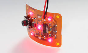
Increasingly common in many modern electronic devices, rigid-flex printed circuit boards (PCBs) offer both durability and flexibility to meet the design requirements of complex electronics. However, these materials do come with their drawbacks, especially in terms of mechanical stress and signal loss. Therefore, engineers and designers must carefully evaluate the benefits of using flex PCBs against their drawbacks to determine whether or not these materials are appropriate for their specific project.
The key to maximizing the versatility of flexible PCBs lies in their structural integrity, which is largely achieved through the use of stiffeners. Stiffeners are adhesive materials that are used to enhance the mechanical stability of flex PCBs, thereby allowing them to withstand bending and folding without losing their original shape or performance.
By understanding the best practices for incorporating stiffeners into flex PCBs, engineers can create robust designs that deliver superior performance and reliability across diverse applications. In order to do so, it is important to identify the factors that influence the effectiveness of stiffeners in a given scenario and understand how these factors can be optimized through various design methodologies.
One of the most essential considerations in designing a flexible pcb is ensuring that all conductive traces are properly routed in a way that maximizes electrical efficiency and signal transmission. This is achieved by routing conductive traces along a path that minimizes impedance variation. In addition, determining an appropriate bend radius is crucial to avoid excessive mechanical stress on conductive traces, which can potentially lead to thinning of copper circuits.

Design Considerations for Flexible PCBs
As with other PCB components, vias are also important to consider in flexible PCB designs. For instance, vias must be designed to withstand excessive mechanical stress in order to maintain their reliability in flexible PCBs. Ideally, it is preferable to avoid placing vias in flex sections of the board, but this may not always be possible depending on the design. In these cases, it is recommended to use “rooms” to define areas that are known to be stationary and use a PCB CAD editor’s design rules to only allow via placement in these regions.
Moreover, it is imperative that all conductive traces in flexible PCBs be routed around the outside of the bend area to prevent short circuits or other problems. In addition, plated through-holes should be avoided in the flex section as they can reduce the effective bend radius of the circuit. Instead, plated through-holes should be placed in the non-flex section of the board.
Finally, when laying out multi-layered flex circuits, it is critical to stagger traces on the front and back of the board. Staggering traces will help to minimize stress contributing to the thinning of copper circuits at the bend radius, and it will increase the overall flex life of the board.
Ultimately, these design considerations are critical for ensuring the longevity and reliability of flexible PCBs. By integrating these optimization strategies into the design process, engineers can create robust rigid-flex PCBs that can be used in a variety of electronic devices.